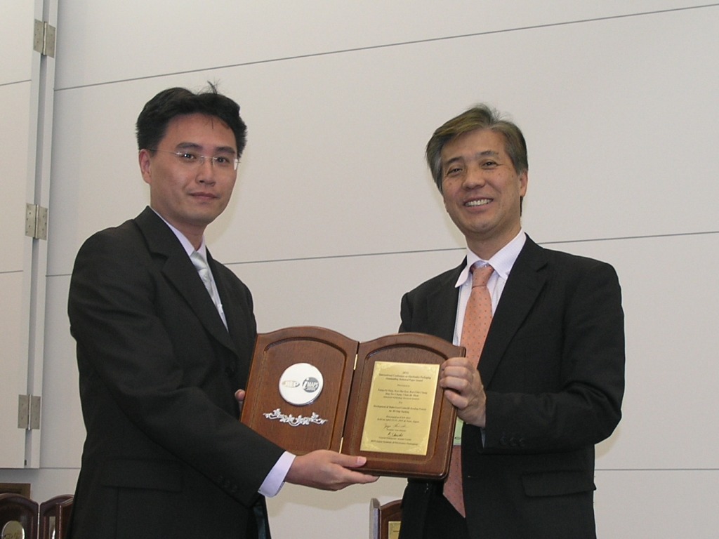
“Development of Wafer-Level Underfill Bonding Process
for 3D Chip Stacking”
T.-F. Yang, K.-S. Kao, R.-C. Cheng, J.-Y. Chang,
C.-J. Zhan
Industrial Technology Research Institute |
 |
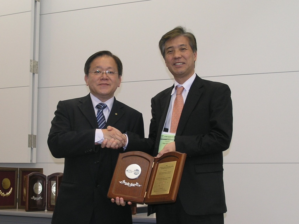
“Investigation of PWB Laminate Resin and Its Relation
with the Pad Cratering Resistance”
C. Yang, F. Song, S. W. R. Lee
Hong Kong University of Science & Technology |
 |
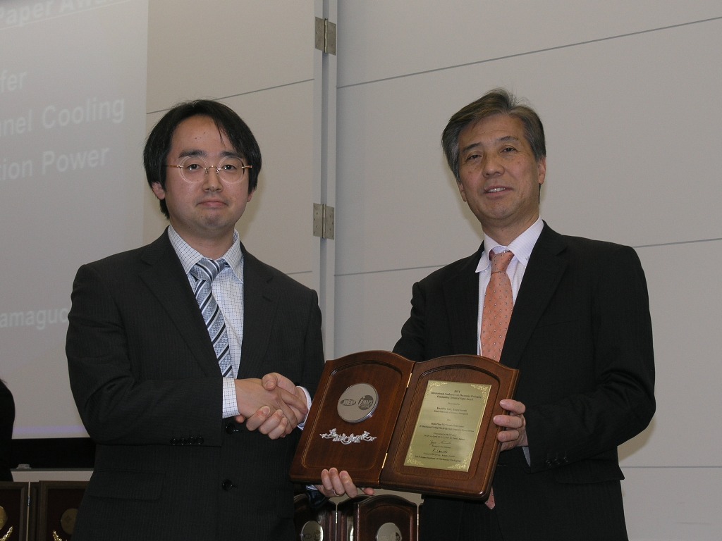
“Single-Phase Heat Transfer Performance of
Minichannel Cooling Fins for the Next Generation Power Devices”
K.
Yuki, K. Suzuki
Tokyo University of Science |
 |
“Silicon
Microparticle Ejection Using Mist-jet Technology”
Y.
Yokoyama1, T. Murakami1, T. Tokunaga1, T.
Itoh1,2
1BEANS Project, 2Reserch
Center for Ubiquitous MEMS and Micro Engineering |
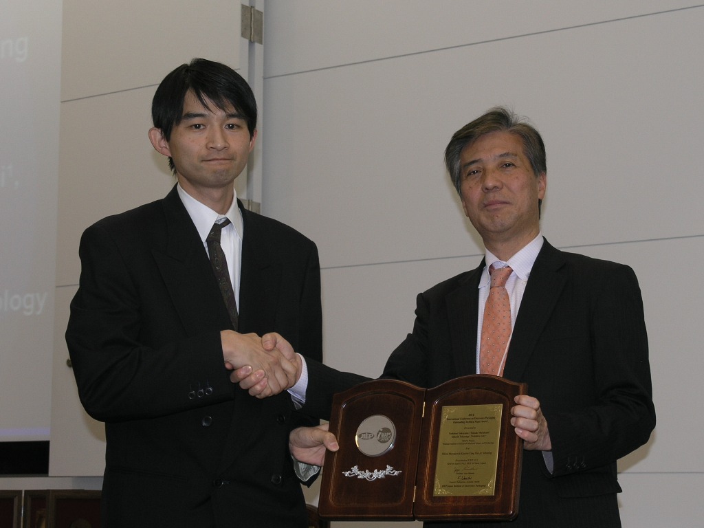 |
“Microstructual Analysis of Wiskers Nucleated from
Lead-Free Tin-copper Plating Films by Mechanical Stress”
Y.
Mizuguchi1, Y. Murakami1, S. Tomiya 1, T.
Asai2, T. Kiga2
1 Sony,
2Sony EMCS |
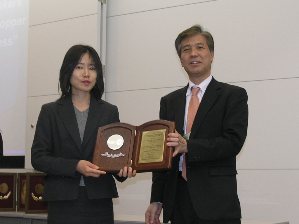 |