2016 Internaitonal Conference on Electronics Packaging
|
|
|

Schedule
| Date | Morning | Afternoon | Evening |
| 20th | Technical Sessions | Award Ceremony / Keynote Lectures |
Welcome Reception |
| 21th | Techninal Sessions | Techninal Sessions | |
| 22th | Techninal Sessions | Techninal Sessions | |
| 23th | Excursion | ||
Keynote Lectures
 |
System Scaling for New Era
of Automotive Electronics – An Ultimate System Integration Opportunity Rao R Tummala Georgia Institute of Technology |
| The new trends in automotive electronics such as autonomous driving, in-car smartphone-like infotainment, privacy and security, and all-electric cars, require an entirely different vision than is pursued today. Georgia Tech sees unprecedented challenges and opportunities to address these needs because of the disparate set of technologies that hitherto fore thought to be impossible to integrate. It proposes a systematic approach to system scaling, heterogeneous integration and innovative package architectures as the new era in electronics hardware with particular focus in electrical, mechanical and thermal designs and new digital, RF, radar, sensors, millimeter wave and power technologies. The Georgia Tech team proposes a transformative, and yet strategic approach, to automotive electronics called System Scaling, leading to an entire automotive system-on- a package. Such a system must integrate many disparate technologies such as high-speed digital, optical, RF and wireless sensing and data processing from 100s of sensors as well as ultra-high power and high-temperature electronics. Georgia Tech proposes highly innovative large panel-based, ultra-thin glass packaging in 3D double-side architecture with many, many innovations in designs, materials, processes, wiring lithography, fine-pitch and highly conductive through-vias and evaporation and condensation for thermal management and nanoscale RF and power components and system integration of all these. Such an approach is proposed to lead to highly-functional and miniaturized systems with disparate set of technologies at lowest cost, in smallest size with shortest interconnections with lowest power consumption. Georgia Tech views this approach to be superior to current approaches such as chip-first or wafer fanout or chip-last organic, leadframe and molded packaging technologies. | |
 |
System Design Challenges
for Future Consumer Devices: from glass to chromebook Eric Shiu Google Inc. |
| Internet and mobile application have been driving force for semiconductor innovation in the past 10 years. It's known that the scaling has been slowing down since 20nm process node. The memory and energy walls have been limiting the end-user's perceivable performance. We will look at the system requirement for the consumer device, such as laptop, phone and glass. Starting from the high-level workloads, such as browsing, video streaming, gaming or taking pictures. Then dive into full-system architecture simulation, performance and power analysis. Finally, a few future research areas in architecture and technology will be discussed. | |
 |
The Frontiers of
Information Technology Dario Gil IBM Research |
| For
decades, computing power has doubled roughly every two years ― a
pattern known as Moore’s Law. Those advances have relied on making
transistors ever smaller, thereby enabling each computer chip to have
more functionality and calculation power. During this time, IBM has
invented many new ways to shrink transistors and fundamental
innovations to improve performance. IBM continues to aggressively
pursue disruptive technologies such as III/V compound semiconductors
and carbon nanotubes for logic devices, magnetoresistive and phase
change materials for memory, and 3D stacking and integrated silicon
nanophotonics for high bandwidth and communications. Still, despite all of these innovative technologies, increasing the density of transistors will cease when length-scales reach atomic dimensions. This raises the fundamental question of what is next? What is the future of information technology beyond scaling and traditional computing? The physical sciences must be marshalled to make matter compute in new ways so that we can create a future beyond Moore’s Law. It is critical to realize that software alone will not deliver sustained exponential speedups. The very nature of computing must be reimagined. Relaxing the constraints imposed by the von Neumann architecture allows for transformational compute methods such as quantum computing and brain-inspired computing extended all the way to the device level. Furthermore, we must create a partnership between people and computers to scale and enhance human expertise. That is the path for all us to make better decisions. The nature of the human-computer interface, and the fluidity of data in and out our bodies and minds, will be transformed. Data must be experienced. And we have to continue our tradition that traces back to Galileo, to make the invisible visible. Whether it is observing molecules down to the subatomic level to understand fundamental properties, observing biological molecules to more quickly understand biological systems, using multiple new segments of the electromagnetic spectrum to create an observing platform that sees in new ways, or looking at data from multiple sources at the geographic length-scale to make new insights and take control actions on a large system, all of these are examples of how technology and data are able to let us see and act in new ways. |
|
Excursion Tour (optional)
Itinerary8:00 Departure from Sapporo
8:20~9:10 Breakfast at the seafood restaurant, Kitano-Ryoba
12:30~14:10 Visit to Mt. Usu
14:20~15:10 Volcano Science Museum
16:40 Arrival at New Chitose Airport
18:20 Arrival at Sapporo
*Please bring your baggage to the excursion if you plan to have a flight from New Chitose Airport on the evening of Apr 23.
 Curb
Market (札幌場外市場, Sapporo Jōgai Ichiba) consists of nearly 64 stores and
restaurants lined up along several blocks just outside of Sapporo's
Central Wholesale Market, where Hokkaido’s fresh seasonal seafood,
fruit and vegetables come together. Kitano-Ryoba
(北の漁場) is one of stores and restaurants in the crab market, and you can
enjoy sashimi-topped rice and sushi etc. [The
photo is
for illustrative
purposes only.]
Curb
Market (札幌場外市場, Sapporo Jōgai Ichiba) consists of nearly 64 stores and
restaurants lined up along several blocks just outside of Sapporo's
Central Wholesale Market, where Hokkaido’s fresh seasonal seafood,
fruit and vegetables come together. Kitano-Ryoba
(北の漁場) is one of stores and restaurants in the crab market, and you can
enjoy sashimi-topped rice and sushi etc. [The
photo is
for illustrative
purposes only.]
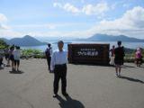 Silo
observatory, located at west side of Lake Toya, is for
overlooking the sparking blue Lake Toya and its island. You can see
Nakajima, Mt. Usu, and Showa-Shinzan all at once.
Silo
observatory, located at west side of Lake Toya, is for
overlooking the sparking blue Lake Toya and its island. You can see
Nakajima, Mt. Usu, and Showa-Shinzan all at once.
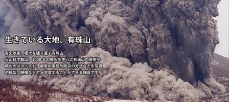 Volcano Science Museum is
a comprehensive learning facility of Mount Usu, which has been erupting
repeatedly since the prehistoric times. Tracing the history of Mount
Usu, the museum introduces the mechanism of volcanic eruptions,
exhibits the actual damages caused by the eruptions in the past, and
shows preventive measures against disasters using photos, models,
diorama, and various other audiovisual materials mainly focusing on the
eruptions in 2000. You can virtually experience what they were like
while learning.
Volcano Science Museum is
a comprehensive learning facility of Mount Usu, which has been erupting
repeatedly since the prehistoric times. Tracing the history of Mount
Usu, the museum introduces the mechanism of volcanic eruptions,
exhibits the actual damages caused by the eruptions in the past, and
shows preventive measures against disasters using photos, models,
diorama, and various other audiovisual materials mainly focusing on the
eruptions in 2000. You can virtually experience what they were like
while learning.
Mount Usu (有珠山 Usu-zan)
is an active stratovolcano in the Shikotsu-Toya National Park,
Hokkaidō, Japan. It has erupted four times since 1900: in 1910 (which
created Meiji-shinzan), 1944–45 (which created Shōwa-shinzan), August
7, 1977 and on March 31, 2000. To the north lies Lake Toya. Mount Usu
formed on the southern rim of the caldera containing the lake. (source:
wikipedia )
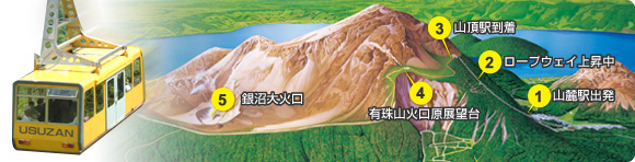
Usu-zan Gondola:
The 6-minutes midair journey affords panorammic views.
1. Depart from Sanroku Station for a 6-minute midair journey (1). A
splendid view of Lake Toya can be seen (2).
2. You’ll see the jagged mountain ahead, and the gondola will soon
arrive at Sancho Station (3).
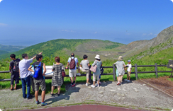
3. Upon arrival, the Lake Toya Observation Deck is on the right,
commanding views of Mt. Showa Shinzan and Lake Toya far below.
4. The Usu Crater Basin Observation Deck is on the left after about a
7-minute walk (4). Passing by the summit (O-Usu), the second summit
(Ko-Usu), and the newest peak (Usu Shinzan) on the way to the Gin’numa
Crater.
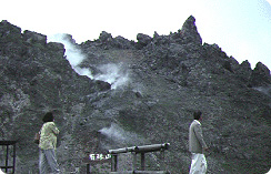
5. The Gin’numa Great Crater formed during the 1977 eruption of the
summit (5). It is the largest of the existing craters. Steam bellows
out continuously. Uchiura Bay can be seen beyond on the Pacific Ocean.
 In August
2009, Toya Caldera and Usu Volcano Geopark was the first in Japan to be
designated as Global Geoparks. Mt. Uus The Geopark has attracted more
worldwide attention.
In August
2009, Toya Caldera and Usu Volcano Geopark was the first in Japan to be
designated as Global Geoparks. Mt. Uus The Geopark has attracted more
worldwide attention.
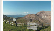
 The view
from the Lake Toya Observation Deck.
The view
from the Lake Toya Observation Deck.
Sponsored
ICEP2016
![]() JIEP (The Japan Institute of Electronics Packaging)
JIEP (The Japan Institute of Electronics Packaging)
![]() IEEE CPMT Society Japan Chapter
IEEE CPMT Society Japan Chapter
![]() iMAPS
iMAPS