
Keynote Lectures
 Heterogeneous Integration - A key enabler for a smart world
Rolf Aschenbrenner
Fraunhofer Institute for Reliability and Microintegration
Abstract:
The digitization process is currently taking place in almost all application areas. Topics like Internet of Things, Industry 4.0 and Artificial Intelligence are an expression of this. In order to support this, electronic systems must become more powerful and multifunctional. Caused by that system integration technologies have to be more variable and application oriented.
Electronics industry has been evolving from a "hardware centric" application to a "user centric" application, leading the electronics system design from a "component assembly" to a "system integration" approach. Therefore two major challenges have to be solved in this context.
On the one hand, Heterogeneous Integration through SiP follows naturally from the conceptual vision to build large, complex systems out of smaller functions separately packaged and require therefore very sophisticated technology platforms (e.g. wafer level or panel level assembly and packaging). At the same time application oriented assembly is very specific and reduces the average of production volumes. That means we need strong modularization and standardization progress covering a wide range of system applications.
In Heterogeneous Integration, an efficient and optimized interplay between the material properties and the packaging technology is especially needed to meet the various application challenges outlined above. An additional difficulty is that partial measuring and testing is generally not possible due to the complexity and tight integration of varying system components. Consequently, successful development is generally only possible if the functional system design, material and technology optimization and design for reliability are coordinated with each other at the beginning of the development process.
Heterogeneous Integration is and will be the key technology direction going forward. It is the high-yield opportunities for initiating a new era of technological and scientific advances to continue and complement the progression of Moore’s Law Scaling into the distant future.
 Design Tools and Modelling Challenges for Heterogeneous Integration
Chris Bailey
University of Greenwich
Abstract:
Advanced packaging and heterogeneous integration of electronic devices requires new developments in design and modelling tools to enable these technologies to meet the requirements for future electronic systems and the benefits these systems will provide such as high data rates, low latency, and massive number of connections. To fully understand the design, materials, and device requirements for these technologies, there is a need for co-design methodologies across the device (Si, GaN, GaAs, etc), package (3D-IC, 2.5d, etc), and board-level/system workflows. This presentation will discuss the current state-of-the-art in co-design with a focus on thermal and mechanical analysis and the challenges that need to be overcome for future electronic systems.
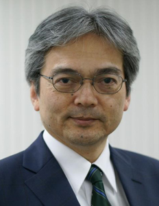 3D Chip Stacking Technologies for the Future
Teruo Hirayama
Sony
Abstract:
We are consciously or unconsciously benefiting from the spread of the Internet of Things. With this spread comes the strong demand for various semiconductors, especially small, multifunctional, and high-performance LSIs. The system on a chip is one solution. However, embedding various technologies on one chip raises the cost of development and of products. Another promising solution is a system in package (SiP) such as a multi-chip 2D or 3D stack package. SiP can easily implement different function chips in a small system without cost issues.
We have so far developed unique 3D stacking technologies to fabricate multifunctional, high-performance, and highly productive devices including image sensors. The potential applications of such devices are infinite. Three example directions for the evolution of image sensors are: improving performance to capture high-quality images with semiconductor technology, taking advantage of photon information that the human eye does not use by developing new materials and structure, and gathering information effectively for decision-making systems. In the very near future, our cutting-edge technology will be key for surveillance, factory automation, autonomous driving, medical imaging, machine learning, etc. I will introduce our past and latest achievements and show the directions of future technology for image sensors using 3D stacking technologies.
 Latest SiP Enabling New System Integration
CP Hung
ASE Group
Abstract:
System in Package (SiP) provides the user the great promise to optimize and differentiate their products to meet their device / system requirements. This talk will review innovations in SiP technologies - Flip-Chip, Fan-Out and beyond, describing how these promises are fulfilled in achieving higher bandwidth, small form factor, with increased functionality and mixed wafer nodes, so comprehensive technologies to the IoT, big data and mobile applications.
 Advanced Packaging Architectures for Heterogeneous Integration (HI)
Ravi Mahajan
Intel
Abstract:
Advanced packaging technologies are critical enablers of HI because of their importance as compact, power efficient platforms. This talk will trace the evolving role of packaging over the past decades and examine its value as an HI platform. Different packaging architectures will be compared primarily on the basis of their physical interconnect capabilities. Key features in leading edge 2D and 3D technologies, such as EMIB, Silicon Interposer, Foveros and Co-EMIB will be described and a roadmap for their evolution will be presented. The talk will conclude with a discussion of opportunities and challenges in driving the package roadmap forward.
 Superconducting circuits for quantum technologies
Yasunobu Nakamura
Research Center for Advanced Science and Technology (RCAST), The University of Tokyo, Japan
RIKEN Center for Emergent Matter Science, Japan
Abstract:
Superconducting circuits are widely investigated for various applications in quantum information technologies these days. Thanks to the drastic improvement of the coherence properties of superconducting qubits in the last two decades, as well as to their large dipole moment and strong nonlinearity that allow fast control and readout, they are considered to be one of the most promising platforms for implementing quantum information processors flexibly designed on-chip. In addition, based on circuit quantum electrodynamics, qubits are coupled to resonators and waveguides to exploit the properties of those bosonic modes, either localized or propagating. In this talk, I will give an overview of the field and introduce our activities.
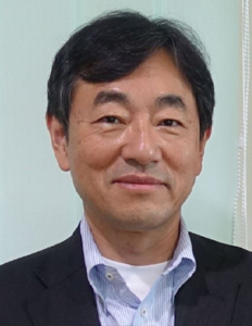 Future trend: Technology merger strengthens evolution of chips in the hyper-scaling era
Kazuya Okamoto,
Yamaguchi University
Abstract:
The industry has historically evolved along an S-shaped growth curve and could be explained by Rogers normal distribution using a diffusion of innovation theory. However, this distribution is changing in the current contestable market created by platformers like GAFA (Google, Amazon, Facebook and Apple). The semiconductor industry, which is a pivotal element of this market, is developing into a new model quite different from the conventional one.
In this keynote lecture, we discuss what a semiconductor should be in the future, based on inductive strategic thinking using intellectual property information and other resources. Specifically, we will review crucial items including: 1) Increased costs to shrink transistors and modify their structures, 2) Transition to 3D to reduce RC delay in the interconnects and create added value, and 3) Need for an optimal solution combining high-density packaging with a chiplet concept.
Today, technology drivers are changing from conventional Memory and Logic devices to AI chips, and the technology merger supports the evolution of these chips.
 Future of Packaging
Madhavan Swaminathan
Georgia Tech
Abstract:
The semiconductor industry is headed towards heterogeneous integration in 2.5D or 3D form being driven primarily by the high cost of monolithic integration. This is great news for packaging. However, given this scenario what should be the "Future of Packaging" in terms of new technologies that need to be developed.
This presentation will use emerging applications in the areas of artificial intelligence, high performance computing, automotive, wireless communication and others as the primary driver to define the packaging requirements along with the current state of the art.

